Research Vision
What We Want to Improve with our Research: The computer chips in every piece of technology we touch are a wonder of innovation, human ingenuity, and minaturization. A single chip will have billions of transistors on it, little switches that store the binary 0’s and 1’s of computer language, which allow the device to render our cute cat videos. However, no one wants a large cell phone.
To pack billions of transistors on a chip that fits in your pocket, each transistor must be ~ 5 nm in size, or 200,000x smaller than a human hair. We have traditionally made these with “top-down” nano-fabrication approaches to chip/material creation, taking bulk pieces of a material and eating away at them (etching, milling, etc.) to produce chips with nm-sized functional elements.
While the past century has seen transformative leaps in methods for top-down manufacturing, the continued drive toward miniaturization has plateaued, with top-down methods encountering fundamental physics limitations in continuing to going smaller. It is clear alternate strategies to enable advanced chip manufacturing or novel material creation must be considered, ideally ones that can preserve the desirable aspects of top-down (fast and mature), while adding new size or performance benefits.
In the Huff lab, we ultimately want to enable the combination of top-down manufacturing with “bottom-up”. In bottom-up, molecular or atomic precursors, the tiniest possible building blocks, are linked together on surfaces into materials with new enhanced function. The Huff lab explores dominantly the bottom-up side, linking atoms together by either:
Bulk techniques like surface self-assembly, where molecules skating around on surfaces assemble into ordered patterns of diverse function.
Atom-by-atom manufacturing using our ultra-sharp probe tips that can “pick and place” atomic building blocks.
Molecules engineered to react in controlled and specific ways with surfaces.
For self-assembly, the pattern the molecules take and its chemical constituents determines its function. Thus, by understanding molecule-surface and molecule-molecule interaction “rules”, we can begin to govern the formation of interesting surface coatings. If one can measure and, eventually, manipulate the rules, one can tailor coatings toward any useful application (photonics gratings, catalysis, oxidation protection, thin conductive chip layers, etc.).
For atom-by-atom atomically precise manufacturing, similar rules must be detailed. How strong is a bond? How can I break it? What will it want to bind to? Can I get more than one reaction product? Building atom-by-atom is the ultimate 3D printer.
Bottom-up processes/understandings developed in the Huff lab are intended to be merged into top-down manufacturing workflows. We partner with other academic and industry partners for the top-down integration work, giving our results broad academic, industrial, commercial, and national value.
Our Broad Research: Our research program aims to detail said fundamental rules for bottom-up manufacturing. If we understand molecules, molecular interaction with surfaces, and molecular interactions with each other, we enable the production of next generation materials. The rules of the molecules/surfaces are detailed by utilization of our unique-in-Canada molecular characterization platform that can measure the structural, electronic, optical, and dynamic interactions of molecules and surfaces at sub-nm resolutions. These include:
Scanning tunneling microscopy (STM) to measure atomic/molecular assemblies and their electronic character
qPlus atomic force microscopy (AFM) to define charge distribution, bond structure, and molecular polarization
Angstrom-resolved tip-enhanced Raman spectroscopy (TERS) to capture dynamic information about molecular flexibility (steric hinderances) and molecule-molecule interactions.
We are also working to bring online ultra-fast time-resolved measurements and photoluminescence studies of single
For more information about the systems, see our Facilities.
Our Research Focuses as of 2026:
Investigate N-heterocyclic carbene (NHCs) molecules on industry-relevant metallic surfaces with qPlus AFM and angstom-resolved TERS. NHCs are exciting for their impact in several semiconductor chip processing aspects like protection during chip layering [1] and smoothing of rough metallic surfaces [2]. We will explore their use for this and detail chemical/electronic/optical properties of their self-assembly patterns.
Build low defect density silicon carbide coatings for quantum material applications using high symmetry tetragem [3] molecules deposited on doped silicon.
Use tetragem molecules to build atomically-precise structures on silicon, targeting quantum defect colour centres [4] for characterization in our optically coupled systems.
Extending qPlus AFM techniques from 2D molecule characterization to 3D molecule characterization.
The above is, of course, flexible and subject to change as we add new members to the group who forge their own research paths in our broad Research Vision.
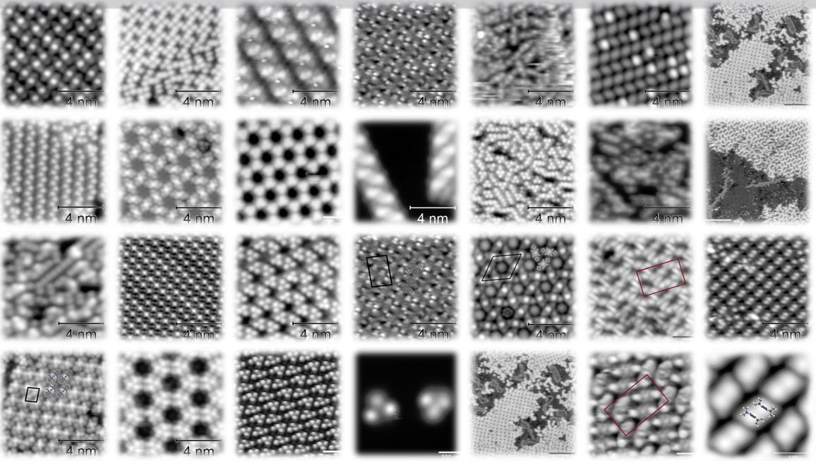
The rich number of N-heterocyclic carbene molecule self-assembly patterns observed on metal surfaces, as measured by scanning tunneling microscopy. Credit: Emmett Desroche

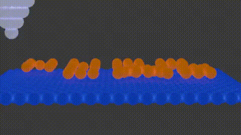
A 32-atom pattern on H-Si(100) made using atomically-precise manufacturing techniques with an scanning tunneling microscope tip.
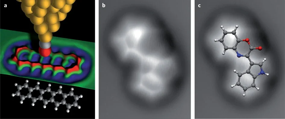
qPlus atomic force microscope image of molecules showing their bond structure. Reference